EU Design Platform DET Vision Paper
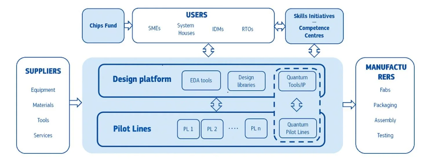
Pillar I of the European Chips Act establishes the Chips for Europe Initiative which has the objective of supporting technological capacity building and innovation in the Union by bridging the gap between the Union’s advanced research and innovation capabilities and their industrial exploitation. The key objective of DETs is to support chip design for Europe’s vast SME OEM base in need of custom silicon innovation. This empowerment is essential for fostering innovation, enhancing competitiveness, and ensuring Europe’s strategic autonomy in critical sectors.
Understanding the needs
The target market of European SMEs present varying needs for DETs. This paper outlines ChipFlow’s proposed solution for a selected segment of European SMEs and OEMs.
Node Diversity Beyond Leading Edge
European OEMs span diverse industries, including automotive, Industrial, IoT and consumer products. The need by the OEMs is not only for the highest process nodes – such as 2nm / 7nm – but it is across a spectrum of nodes from the leading edge all the way to legacy nodes.
As an example, Automotive industry will be in a great need of 90/130nm solutions for a large portion of Software defined vehicle (SDV) driven zonal architectures. To have a low-cost solution to the area is a critical enabler to support European OEMs and their suppliers.
2. Low-Volume Requirements
SME OEMs typically operate with production volumes starting from tens of thousands of units per year, making the design costs a significantly larger part of the overall cost than when compared with larger production volumes.
To support SMEs in the early stages of the product lifecycle, prototyping and production costs at low volumes need to be reduced below current industry norms. The Design Platform initiative helps to reduce the costs for the OEMs but it is only a subsidy and hence more long term solutions need to be fostered.
3. Existing Skills Support
Many OEMs lack in-house ASIC design expertise. Effective design partners must bridge this gap by offering innovative design environments and make it easier for non-ASIC designers. SMEs need to avoid reliance on costly ASIC contractors or continue to rely on unoptimized off-the shelf solutions. OEMs require DETs that evolve with their product lifecycles, enabling them to incrementally build hardware IP assets from initial prototypes to production-grade chips.
The ChipFlow solution
ChipFlow brings a true software/hardware co-design approach to the European market. By using a Python-based flow, ChipFlow enables SMEs to utilise their existing software expertise, to create custom hardware for required applications. ChipFlow is collaborating with a range of wafer fabs to explore flexible manufacturing options that can be tailored to various volume and node requirements.
Flexible ASIC design support
The solution enables both DIY and Design House mode.
DIY Mode: OEMs can independently design their chips using ChipFlow’s intuitive tools, fostering in-house capability development and reducing the need for expensive ASIC designer capability.
Design House Mode: ChipFlow can act as a design partner, allowing OEMs to outsource the process initially and transition across to DIY mode as their internal expertise grows.
Optimised cost structure
ChipFlow’s Cloud flow has 2 tiers - Free and Commercial.
Free-to-Use Tier: A truly open-source platform that democratizes chip design by providing accessible tools for experimentation and learning.
Commercial Tier: A professional-grade option tailored for OEMs focused on delivering commercial chips. The ChipFlow solution will remain affordable even after EU Chips Act based subsidies finish.
Full product life-cycle support
The end-to-end solution - EDA and Supply Chain flow - is ChipFlow’s vision designed to cover all product innovation stages.
Test chips: Choose from 3 leading fabs to find the best process node fit.
Production chips: A unique, pre-integrated offering of:
Foundry A (1-3k chips)
Foundry B (legacy based range for 100k to millions of units)
Foundry C (full range for 100k to millions of units).
How does ChipFlow compare?
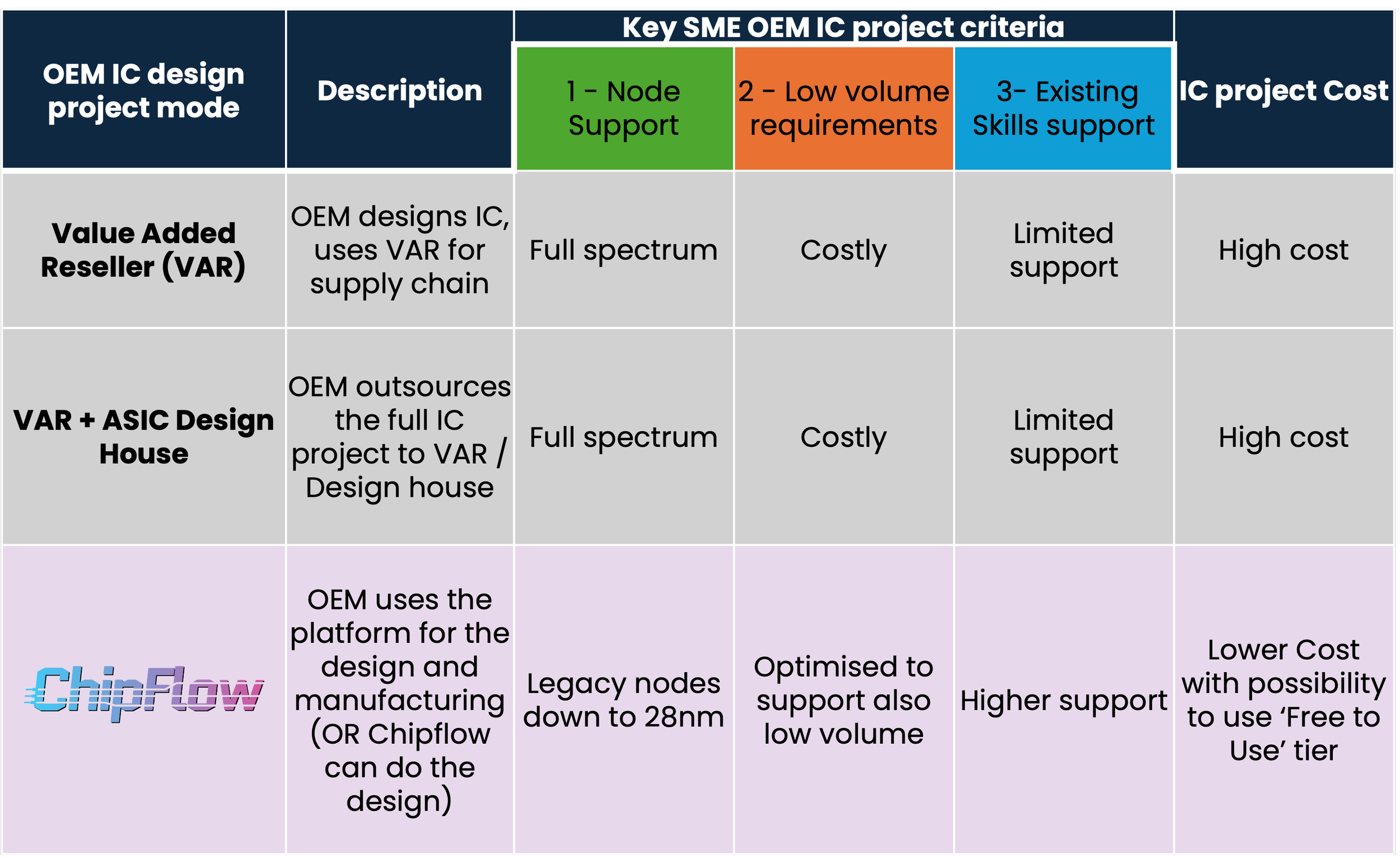
ChipFlow’s end-to-end model adds a new option for OEMs who are considering an IC design project. The IC design project avenues by Value Added Resellers & ASIC Design Houses are well established and support OEMs with larger volumes and existing capability to manage an internal ASIC portfolio. However, as discussed above the ChipFlow model brings advantages targeted to Small and Medium sized (SME) OEMs with fewer resources.
Furthermore, ChipFlow’s model is tailored to significantly lower the cost of IC development projects to make them affordable even for SME OEMs.
The table below summarizes how ChipFlow and its Supply Chain partner solution compares with existing industry standard based DET combinations.
In summary, ChipFlow DET proposition is uniquely designed to support an SME OEM with no previous ASIC design experience. The tiered model enables OEMs to test it without cost while the Python based design approach enables the leveraging of existing in-house talent. Finally, the pre-integrated Supply Chain partner network provides an ample offering to choose from for test through to full production chips.


